Electron Microscopy Laboratory
Electron Microscopy Laboratory
Scanning electron microscope is a device designed to produce high spatial resolution images of the surface of the object.
The possibilities of scanning electron microscopy are used in all fields of science and industry, such as biology, biomedicine, geology, paleontology, physics, nanomaterials, material sciences and others.
The principle of scanning electron microscopy: electron probe (electron beam) is directed to the analyzed sample. The interaction between the probe and the sample electronically generates low-energy secondary electrons which are collected by the secondary electrons detector. The intensity of the signal depends on the nature of the sample (less) and on the topography (more) in the interaction region. Thus, the electron beam scans the surface of the object and obtains the relief map of the analyzed area.
Thin electron probe is generated by an electron gun, which acts as a source of electrons, and focuses by the electron lenses (electromagnetic, electrostatic). Scanning probe coil is deflected in two mutually perpendicular directions and scans the surface of the sample probe. The electron source, electron lenses (toroidal magnetic) and deflection coils form a system called electron column.
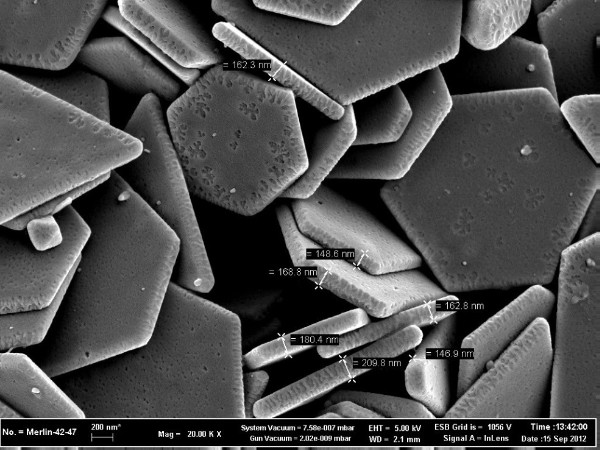
All this features are represented by field emission scanning electron microscopy multipurpose analytical complex Merlin (Carl Zeiss).
Also, this unit is equipped with additional detectors:
Merlin is equipped with energy-dispersive spectrometer that allows elemental analysis and mapping. The electron backscatter diffraction crystallographic detector gives full information on the structure of the sample, for example, the crystallographic orientation of the grains, the definition of the unit cell parameters, mapping of the orientation of the crystal grains.
The possibilities of Merlin analytical complex:
- The surface morphology with a 0.8 nm resolution
- Microprobe elemental analysis
- Construction of phase contrast maps
- Crystallographic objects local structural analysis


Transmission electron microscopy (TEM) involves the study of thin sections or objects with the help of an electron beam passing through them and interacting with them. Due to lower than the light wavelength of the electron TEM allows to study samples with the tens of thousands of times superior resolution then the most advanced optical microscope. TEM makes possible studies even at the atomic level. TEM is a major research method in a lot of application areas: physics, bio-medicine, chemistry, mineralogy, materials science and nanotechnology. Modern TEM units allow studying the elemental composition of the samples and the orientation of the crystals.
Hitachi HT7700 Exalens transmission electron microscope can operate in the following modes:
-Bright Field (contrast is formed by the electron absorption model)
-Dark Field (contrast depending on atomic number)
-Diffraction Contrast (microdiffraction)
-element Mapping using energy-dispersive X-ray spectrometer.
Atomic resolution transmission electron microscopy complex to study nanoscale objects Hitachi HT7700 Exalens


